Perovskite is the next big thing when it comes to solar energy research methods, as it may just have the ability to convert light into electricity in a more efficient and cost-effective way, potentially changing the landscape of the solar industry.
When compared to the silicon semi-conductors used today, these amazing crystal structures have impressed the scientific community to no end, as they can be created quite inexpensively while being utilised within various applications such as LEDs, solar cells and possibly even in phones and computers.
Such feats are astounding in its entirety, however new research by University of Oxford and University of Washington published in the Science Journal has indicated that this material, previously believed to be uniform, may have flaws in them that can be utilised to further improve solar devices and usage.
Perovskite VS Silicon
Dane deQuilettes, a UW doctoral student, working together with Professor of Chemistry and Associate Director of the UW’s Clean Energy Institute, David Ginger, has stated that perovskites are the most rapidly growing types of PV material over the past few years. In quite a short time, this material has managed to convert light into electricity and is fast catching up to the current most used silicon type solar cell technology, that took almost five decades to create.
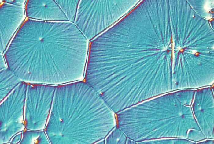
The team applied extremely high powered techniques when it came to their imaging in order to locate any defects within the films of the material which would limit movement changes and thus the overall efficiency of the device.
Perovskite cells have managed to reach 20 per cent efficiency, compared to the 25 per cent for silicon types of cells.
Through a partnership with the Clean Energy Institute researchers were able to utilise a specific technique called confocal optical microscopy, commonly used in biology, which is applied as a semi-conductor technology. Using florescent pictures and correlating them by electron microscopy images, they could locate the darker performing areas within the material intersections of the crystal. By using this method they also discovered that they were able to activate certain parts of the poorly performing areas using a very simple chemical treatment.
Utilisation of perovskite material expected to advance further
The images had many surprises in store for the team which will no doubt lead to improvements within the uniformity, efficacy and stability of the material. Such results prove that even though this material is amazing and highly-efficient, it still can be improved upon which gives a better start for future research teams to work upon and enhance the materials.
This imaging solar energy research technique used by the UW research team is a simple way to locate undiscovered flaws within the perovskite crystal and also point out any regions where its make-up may be treated in a chemical manner in order to boost its performance further.
deQuilettes has stated that he thinks over 1000 labs the world over are researching the semi-conducting nature of perovskite materials, however much more work is needed in order to understand how to allow the material to be stable with uniform brightness and having it withstand moisture without it degrading.
The new UW study has allowed for out-of-the-box thinking on how to better the materials as well as how to utilise them within other types of applications such as high-performance devices like lasers and LEDs.
With this much attention on perovskite materials, this new technique will definitely shine light on steering researchers towards the best places in order to maximize its energy harvesting and emitting characteristics.


